

- Thin film resistor networks offer outstanding precision, stability, and tight tolerance needed in high-end electronics.
- Their design enables ultra-precise ratio matching by fabricating resistors simultaneously on a single ceramic substrate.
- Laser trimming and careful material selection enhance accuracy, optimizing performance for critical measurement instruments.
Starting with the keyword itself—thin film resistor—these components are the unsung heroes in the world of precision electronics. Whenever you're dealing with circuits demanding high accuracy, low noise, and exceptional stability, thin film resistor networks often form an essential foundation.
When you think about resistors in electronics, the primary function is simple: resistors limit current or divide voltage. But thin film resistors bring this concept to a whole new level, particularly in sensitive measurement devices like high-end multimeters or audio equipment.
What Is a Thin Film Resistor Network?
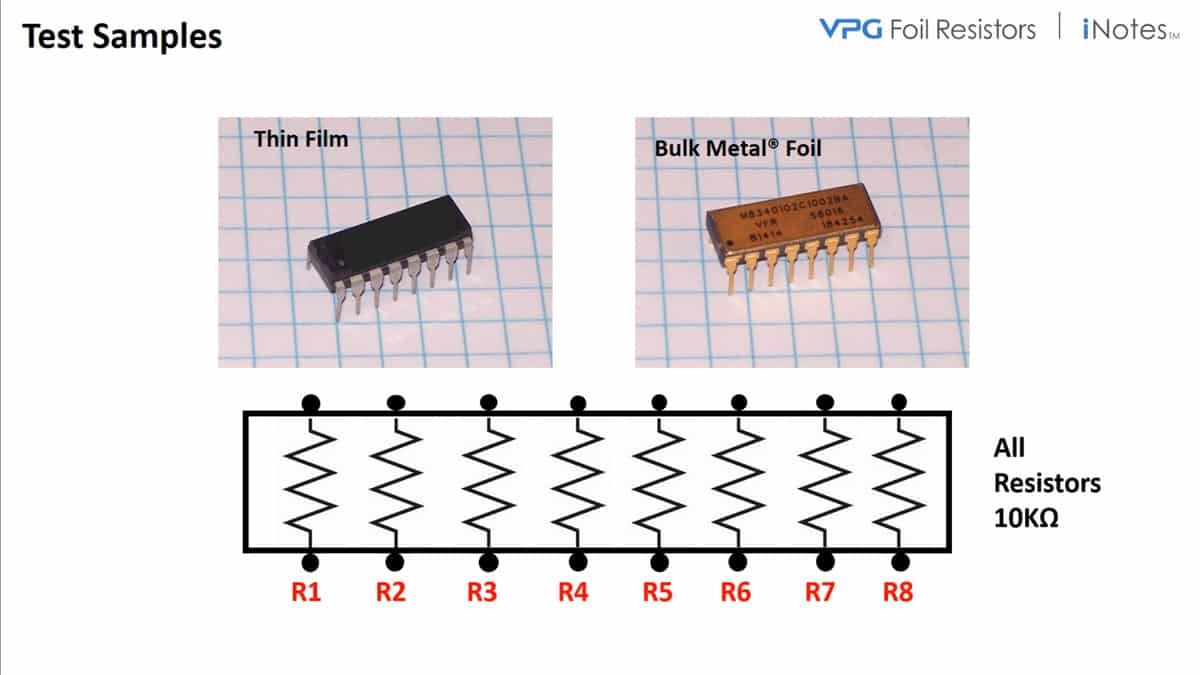
A thin film resistor network consists of multiple thin film resistors integrated onto a single substrate, usually ceramic. This integration provides excellent matching and thermal tracking, because all resistors share nearly identical conditions — temperature, mechanical stress, and aging factors. This is critical when you need accurate ratio measurements rather than just absolute resistance values.
The resistive element is a very thin layer of a metal alloy — commonly nickel-chromium (nichrome) — deposited through a vacuum sputtering or evaporation process onto a ceramic base. This film is typically less than one micron thick, patterned with photolithographic techniques, then laser trimmed to reach exact resistance values.
How Thin Film Resistor Networks Are Made
The manufacturing process is quite fascinating and sophisticated:

- Start with a ceramic substrate, chosen for its temperature stability and minimal expansion characteristics.
- Deposit a uniform thin film of nichrome or a similar alloy via sputtering.
- Use photolithography to pattern the resistive paths, forming traces and serpentine shapes.
- Laser trim the resistors individually to fine-tune each resistor's value by removing small amounts of resistive material. This step is subtractive—which differentiates thin film technology from thick film, where resistive paste is screen printed (an additive process).
- Finally, protect the entire network with a hermetic glass or epoxy layer to prevent moisture ingress.
This glass hermetic sealing is especially important in precision instruments, safeguarding against environmental factors that could cause drift over time.
This complex but precise process yields resistors with:
- Low temperature coefficients (often just a few parts per million per degree Celsius),
- Excellent ratio matching,
- Tight tolerance (sometimes down to 0.01%),
- Low noise performance,
- And stability over years.
Thin Film vs Thick Film Resistors: What’s the Difference?

Often confused with thick film resistors, the difference lies both in construction and performance:
- Thickness: Thin films are less than 1 micron thick; thick films are usually 10 microns or more.
- Process: Thin film uses vacuum deposition and photolithography with subtractive laser trimming, while thick film uses screen-printed conductive and resistive pastes baked onto the substrate.
- Precision: Thin film resistors consistently outperform thick film in accuracy, temperature coefficient, and long-term stability.
- Cost: Thin film resistors cost more due to the complexity and precision of manufacturing, so they are reserved for high-end or sensitive applications.
Why Use Networks Instead of Single Resistors?
You might wonder why manufacturers integrate multiple resistors in one package. Here are the main reasons:
- Ratio Accuracy: In voltage divider circuits, the relative ratio between resistors is often more critical than their absolute values. Networks ensure all resistors share the same process, minimizing mismatch.
- Thermal Tracking: Because all resistors are on the same chip, their temperature-induced variations happen uniformly, keeping their ratio stable.
- Reduced Size and Assembly Effort: Instead of placing many discrete resistors, networks reduce component count and simplify PCB layout.
- Reliability: Networks have robust construction and easier handling, reducing the risk of soldering failures compared to multiple discrete components.
Typical Applications
Due to their performance, thin film resistor networks have become staples for:
- Precision measurement tools (bench multimeters, calibrators),
- Medical equipment,
- Audio devices requiring low noise and distortion,
- Aerospace and military-grade electronics,
- High-frequency circuits needing low parasitic inductance,
- And sensitive sensor interfaces.
For instance, in a high-end benchtop multimeter, thin film resistor networks provide the extremely stable voltage dividers essential for precise voltage readings, often with tolerance and stability better than 10 ppm (parts per million).
Laser Trimming and Ratio Stability
A remarkable manufacturing step is laser trimming. After the initial film deposition and patterning:
- The resistor value is measured in real time.
- A laser ablates tiny amounts of resistive film to adjust resistance upward (you can only add resistance by trimming).
- Various trimming patterns like linear cuts, ladders, or serpentine shapes provide incremental adjustments for ultra-fine tuning.
This approach lets manufacturers tailor resistors to exact target resistances and achieve excellent long-term stability of resistance ratios.
Key Points to Remember
- Precision Thin Film Resistor Networks are critical for high-accuracy and stable electronics.
- Their manufacturing involves sophisticated thin film deposition and laser trimming on ceramic substrates.
- The networks deliver outstanding ratio matching and temperature tracking compared to discrete resistors.
If you want to dive deeper into their internal structure or manufacturing, manufacturers like Vishay and Susumu offer detailed technical documents and design guidelines. For practical examples and teardown insights, specialized electronics channels provide excellent hands-on videos.
FAQ Section
Q: What makes thin film resistors more precise than thick film?
A: Thin film resistors use a vacuum-deposited, very uniform conductive film patterned photolithographically and adjusted by laser trimming, leading to tighter tolerances and lower temperature drift compared to additive thick film resistors.
Q: Can I use thin film resistor networks for power applications?
A: Typically, thin film resistor networks are designed for low to moderate power applications where precision is more important than power dissipation. For high power, specialized thick film or wirewound resistors are preferred.
Q: Are thin film resistor networks expensive?
A: Yes, they tend to cost significantly more than standard thick film or discrete resistors due to their complex manufacturing process and precision. They are justified in applications requiring high stability and accuracy.
Q: What is the advantage of laser trimming?
A: Laser trimming allows fine adjustment of resistance values after fabrication to meet exact specifications and stabilize resistor ratios critical in precision circuits.
Q: Can thin film resistor networks be damaged by moisture?
A: Moisture can affect the resistance and reliability, which is why hermetic sealing with glass or epoxy films is crucial to protect thin film networks.
For more on thin film resistors, visit sites like EEPower and Korvus Technology, which provide excellent technical overviews and applications.

%20(1)%20wepb.webp)
